
ASE has developed the industry’s first automated 310mm panel-level packaging production line, targeting production in the first half of 2027 to meet surging AI and HPC demand.
Manufacturing breakthrough
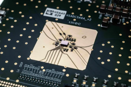
The new line moves beyond traditional round wafers to rectangular 310mm × 310mm panels, yielding up to 96,100 mm² of usable area per panel. This shift enables significantly more dies per unit and improves material efficiency, directly addressing the rising interposer sizes and declining wafer-level efficiency that challenge current advanced packaging.
ASE’s platform supports line/space capabilities of 2/2µm for its FOCoS technology and 8/8µm for FOCoS-Bridge, maintaining design rule consistency across both platforms. The automated line reduces tool change steps and cycle times, offering higher throughput for complex multi-die architectures.
Heterogeneous integration enabler
As AI accelerators and HPC devices scale toward trillion-transistor system-in-package designs, high-bandwidth, low-latency interconnects between chiplets, ASICs, and HBM become critical. Panel-level packaging provides the larger format and higher I/O density needed for these architectures, supporting applications from AI data centers to high-end gaming and edge AI.
“This innovation enables higher integration density and supports the evolving requirements of AI and HPC systems, where performance, power efficiency, and manufacturability must be addressed holistically,” said Dr. C. P. Hung, ASE’s Vice President of Corporate R&D.
Competitive positioning
The panel line reinforces ASE’s differentiation through faster cycle times and scalable manufacturing aligned with chiplet-based roadmaps. Executive Vice President Yin Chang noted that hyperscale customers are driving the pace of innovation, requiring advances in packaging efficiency alongside silicon improvements.
ASE will showcase the platform at the 76th IEEE ECTC in Orlando, May 26–29, 2026. CEO Dr. Tien Wu will deliver the plenary keynote on advanced packaging and system optimization.
Outlook
Panel-level packaging marks a pivotal step beyond wafer-based processes, enabling the throughput and integration density required for next-generation AI and HPC systems. ASE’s automated line positions it to lead this transition, offering customers a scalable path to higher performance with improved manufacturing efficiency.