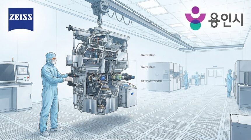
Zeiss Semiconductor Manufacturing Technology (SMT) has opened a new innovation center in Yongin, Korea, expanding its footprint in one of the world’s most critical chip markets.
Why Korea and why now
The facility integrates Zeiss’s Semiconductor Mask Solutions and Semiconductor Fab Solutions portfolios, focusing on high-precision metrology, inspection, and mask repair technologies. Its mission is to support innovation in high-volume wafer production and advanced packaging applications.
Key systems installed at the center include:
– **NLX®-100**: a 3D X-ray metrology and inspection solution that provides high-resolution diagnostics on complex package structures, enabling process control for wafer-level and advanced packaging.
– **DUNE®100**: enables active wafer shape control with integrated high-precision metrology, allowing fabs to measure and correct global wafer warpage individually at every critical step.
– **MeRiT® AE**: a next-generation mask repair technology designed to address the most critical and smallest defects on photomasks while maintaining high yield—essential for advanced semiconductor processes.
Zeiss plans to add more solution equipment to the center to strengthen early technical cooperation with Korean customers.
A shortcut from problem to solution on the factory floor
The innovation center functions as a collaborative platform for direct engagement with leading Korean chip manufacturers. Dr. Frank Rohmund, President & CEO of Zeiss SMT, stated, “We are pleased to open our first global Semiconductor Innovation Center in Korea, as one of the key locations for the global chip industry. With this center we are moving Zeiss closer to our customers.”
The facility enables on-site development, process optimization, and faster qualification for high-volume production environments, accelerating the transition from research and development to customer adoption. Dr. Jaane Seehusen, future Head of Zeiss Korea, noted, “The Innovation Center in Yongin is an important step in our strategy to strengthen customer interaction in the semiconductor industry and additionally Zeiss’s overall presence in Korea.”
The quiet shift in the global chip supply chain
This investment underscores Zeiss’s commitment to deepening its presence in Korea, a pivotal semiconductor manufacturing hub. By providing local access to advanced metrology, inspection, and repair technologies, Zeiss positions itself as a long-term partner for Korean chipmakers navigating increasingly complex process nodes and packaging demands.
As the semiconductor industry pushes toward finer geometries and heterogeneous integration, the ability to rapidly deploy and refine precision tools on-site will be a competitive differentiator. Zeiss’s Yongin center is a clear signal that the company intends to be at the forefront of that shift.