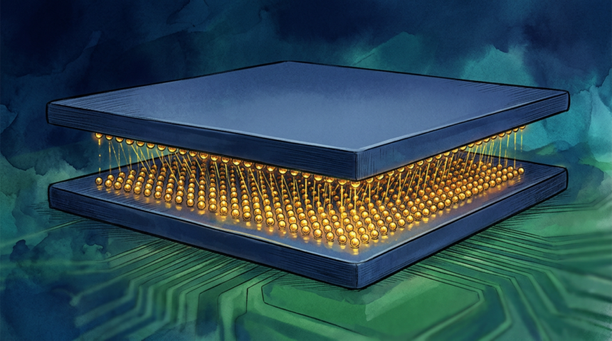
The bonding method that joins memory to AI processors is staying put for now, and TSMC is spending to make it smaller. DigiTimes reported September 2, citing ETNews, that the foundry has asked materials and equipment vendors to develop 5-micron-class microbump bonding with matching underfill for advanced HBM packaging.
TechPowerUp framed the same development as a delay in TSMC’s hybrid-bonding investment for HBM in favor of conventional microbumps. Underfill, the material that fills the space between stacked dies, is central to the challenge because finer bumps leave less margin during reflow and thermal cycling.
Hybrid bonding has long been described as the endgame for stacking memory directly on logic, replacing solder entirely with copper-to-copper joints at far tighter pitches. The switch demands new equipment, new materials and a fresh yield learning curve, so suppliers are being lined up to extend the microbump roadmap first.
TSMC’s choice reverberates across the supply chain. The foundry packages the HBM used in the AI accelerators driving the memory boom, and its process decisions help set the pace for equipment and material makers in Taiwan, Japan and Korea. If 5-micron microbumps prove reliable in volume, the expensive hybrid-bonding buildout for HBM could slip by years and reshape the packaging roadmaps suppliers have been planning around.