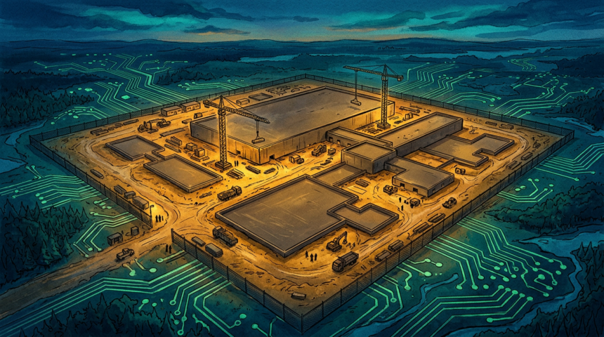
SK hynix has broken ground on its first US high-bandwidth memory plant, a $4B advanced packaging facility in West Lafayette, Indiana, that will start producing HBM4E in the third quarter of 2029.
The ceremony on August 27 at Purdue Research Park drew Indiana Governor Mike Braun, Senator Todd Young and interim Purdue president Mitch Daniels, alongside CEO Kwak Noh-Jung. The company also signed a partnership framework with Purdue covering advanced packaging research and development.
The plant, first announced in April 2024, will combine a next-generation HBM packaging line with an AI memory research facility, and is expected to support roughly 1,000 employees when production ramps. Cleanroom operations are scheduled for the second half of 2028, with advanced wafers from SK hynix fabs in South Korea shipped to Indiana for packaging and testing before delivery to US customers.
Kwak used the occasion to address the memory market, saying the current chip shortage should last through the end of 2030 with no clear signs of a downturn. He added that annual capacity at the site could eventually climb into the hundreds of thousands of wafers, and left the door open for more US spending. On the Solidigm NAND unit’s planned US IPO, Kwak said the listing remains under discussion.
The project puts advanced HBM packaging on American soil close to Nvidia, Microsoft and Google, part of a broader push by Washington to pull memory manufacturing and packaging into the US.