
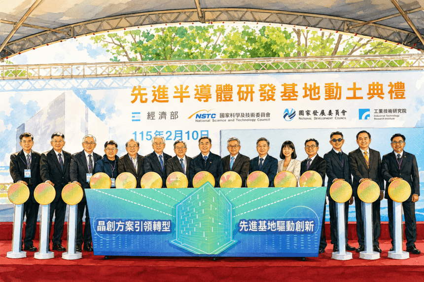
Taiwan just dug the foundation for its most ambitious semiconductor gamble yet. The Ministry of Economic Affairs broke ground this week on a new R&D center in Hsinchu that will house the island’s first 12-inch pilot line—a dedicated testbed for the next wave of chip technology. Think AI accelerators, silicon photonics, and quantum computing hardware.
The 12-Inch Bet
This isn’t just another fab expansion. The facility, backed by the IC Taiwan initiative and a NT$3.77 billion investment, is designed to bridge the gap between lab experiments and factory floors. Right now, startups and SMEs often get stuck in the “valley of death”—their novel designs work in theory but can’t afford the verification runs on commercial lines. This pilot line changes that. It will handle 28-90 nanometer back-end-of-line (BEOL) processes, the crucial final steps where chips get their interconnects and packaging.
One-Stop Shop for the Future
Minister Kung Ming-hsin framed it as a complete ecosystem play. The center will integrate design verification, advanced process development, and equipment validation under one roof—covering design, manufacturing, packaging, and testing. That’s a direct response to Taiwan’s 8.36% GDP growth last year, which was largely powered by semiconductors and AI. The goal? Slash product development cycles by about 30%.
Construction wraps in December 2027, with operations starting in Q1 2028. But the real deadline is existential: Taiwan needs to stay ahead as the US, Japan, and Europe pour billions into their own chip ecosystems. This pilot line isn’t just a lab—it’s a hedge against obsolescence.