A silicon photonics chip has a component problem, and Kyocera may have laser-cooked its way past it. Working with Tohoku University, the company built optical isolators straight onto photonic dies using a localized heating step.
The isolator’s job is one-way traffic. Light travelling backwards into a laser spoils its output, which is why packaged optics need the part at all.
Co-packaged optics raise the stakes, since they deliberately fold optical and electrical circuits into a single package to shorten signal paths. That design wants the isolator grown on the die rather than attached afterward.
Heat was always the blocker. A magneto-optical garnet only functions once it has been treated at roughly 600C or above.
Run a whole wafer through a furnace at that temperature and the wiring, electrodes and everything else already patterned into the chip suffers. The garnet cannot simply be added last under those conditions.
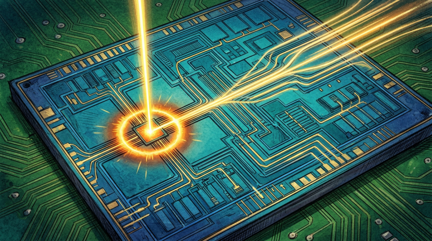
The alternative the two partners developed applies heat with a beam, confined to the small areas where garnet is needed while the surrounding device stays cool. Researchers at the university’s Research Institute of Electrical Communication showed the device operating.
A paper out of the team, dated September 2, describes the demonstration. It ran in IEEE Access.
Silicon photonics has attracted serious money as generative AI loads up data networks, yet the isolator had stubbornly resisted on-chip integration. Fabricating it monolithically would eliminate a separate part from the assembly line.