Making silicon transistors smaller keeps getting more expensive. Gates that narrow bring leakage, heat and power losses with them, which is why labs have hunted for years for materials that carry current better at the atomic scale.
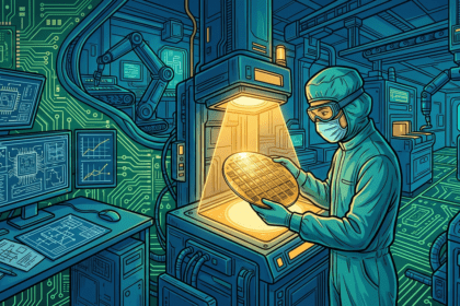
Nexstrom, incubated in Singapore by Xora Innovation, is betting the answer is to put such films onto production lines rather than leave them in labs. North Star, its product, grows transition-metal dichalcogenides straight onto 300mm wafers, the format commercial fabs already run.
The company has taken $12 million in seed funding to push the approach toward commercialization. TMDs sit only a few atomic layers deep, and that thinness is what makes them a candidate channel material once silicon stops scaling.
Others are chasing the same ground. TSMC, Intel and Belgium’s Imec all have programs aimed at integrating 2D materials into transistors, and on the equipment side AIXTRON works on a different piece of the puzzle. A recent demonstration by TSMC, ASML and Imec used 300mm wafers to build transistors from 2D-material films.
The bottleneck sits in deposition rather than in the material itself. Holding uniformity and defect density steady across a whole wafer is what decides whether a laboratory result survives contact with a fab. Timing helps the pitch, too: a memory-driven component shortage has revived appetite for process routes that promise more performance without paying for another lithography node.