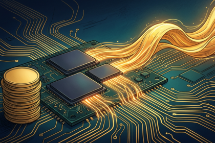

Microsoft used the OCP Global Summit to unveil Maia 300, the third generation of its in-house accelerator, and said the family will scale to multi-gigawatt deployments from 2027.
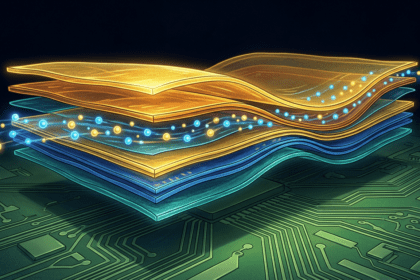
Scott Guthrie, who runs Cloud and AI, framed the part as a complete system rather than a chip. Its compute chiplets are built on TSMC’s N2P node, splitting compute, memory control and input-output into separate dies.
Memory is where the numbers land. Eight HBM4 stacks feed 18 TB/s of peak bandwidth inside a 950-watt envelope.
Microsoft says the design yields 40 percent more tokens per megawatt than leading GPU systems, and up to seven times the rack-scale throughput of Maia 200 in a 96-accelerator configuration.
The bet is that inference, not training, decides who controls AI economics. Long-context reasoning and multi-step agents spend their time moving data, so the company treats dataflow as a first-class design principle, keeping values local and cutting movement between compute, memory and network.
That is the same logic behind a broader industry pivot toward inference-optimized silicon, where memory bandwidth and energy per token matter more than raw floating-point throughput.
The risk is supply. Moving to N2P couples Microsoft’s roadmap to TSMC’s newest and most expensive node, at a moment when leading-edge capacity is already contested.
When Maia 300 enters production in 2027, it will test whether a hyperscaler can genuinely substitute its own design for merchant GPUs at gigawatt scale.