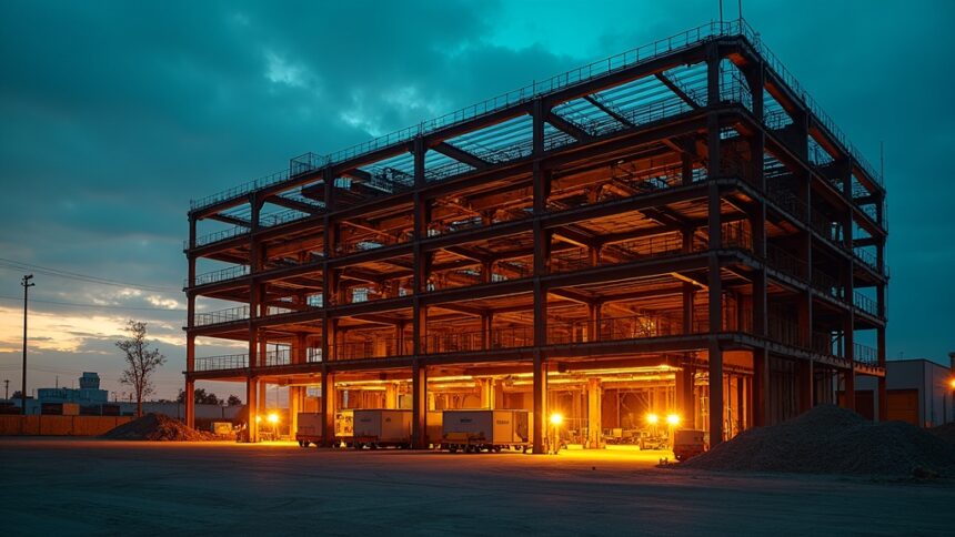
Intel has officially broken ground on a late-stage expansion of its Bowers Campus in Santa Clara, California, dedicated to next-generation EUV mask manufacturing capacity, according to reports from Wccftech and the San Francisco Business Times.
The expansion project spans a 107,000-square-foot site and includes two three-story buildings dedicated to manufacturing, fabrication, and central utility operations. The development was originally scheduled to begin in mid-2026, keeping the timeline on track.
Policy timing adds pressure to the buildout schedule. Semiconductor and advanced manufacturing projects must break ground by December 31, 2026 to qualify for the 35% Investment Tax Credit under the CHIPS Act. Intel’s Santa Clara groundbreaking meets this window.
Meanwhile, Intel’s Fab 52 at the Ocotillo campus in Chandler, Arizona, entered full-scale production in October 2025 as the company’s first high-volume EUV facility. The fab is designed to support more than 10,000 Intel 18A wafer starts per week, translating to roughly 40,000 wafer starts per month at full ramp. The next major Arizona expansion phase would be Fab 62, expected to enter production around 2028 with flexibility for either 14A or 18A process technology.
Intel’s Ohio project remains the most delayed in the pipeline, with Phase 1 completion pushed to 2030.