France’s CEA-Leti is pushing a 3D integration roadmap it says is essential as AI models outgrow today’s memory and power budgets. Pascal Vivet, program manager for advanced programs, told EE Times that moving from high bandwidth to wide bandwidth is the goal: stacked DRAM beside the processor, as in HBM, is no longer enough.
“HBM means high bandwidth, but it’s not wide enough,” Vivet said. The institute wants slower, wider, closer interfaces, with memory placed directly above compute using denser, lower-energy connections. The target: hundreds of gigabytes to terabytes of memory integrated near the chip within a few years.
Leti’s toolbox spans 10-micron-class interconnects down to below 1 micron, including die-to-wafer and wafer-to-wafer hybrid bonding, ultra-dense through-silicon vias, and fan-out wafer-level packaging. The institute recently demonstrated die-to-wafer hybrid bonding at 1-micron pitch and targets 200 nm for wafer-to-wafer.
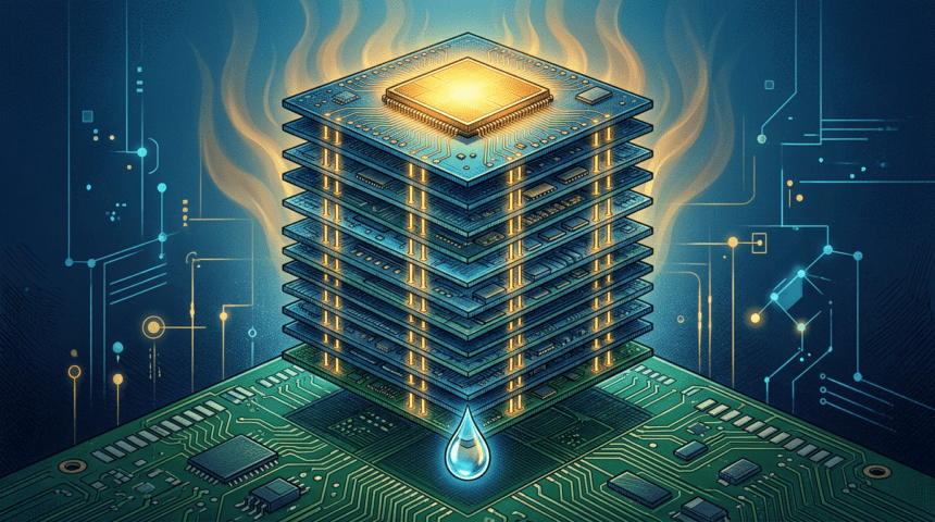
The obstacle is power density, not total power. Stacking concentrates heat, and water cooling sets the ceiling. Wider, slower interfaces cut energy per bit, and power delivery must be re-architected early, with backside delivery as a first step.
Vivet argues packaging decisions can no longer wait until after circuit design. Early partitioning, virtual prototyping, and cost modeling are needed before the physical architecture is locked.