Applied Materials and TSMC have announced a joint innovation partnership at Applied’s new EPIC Center in Silicon Valley, targeting the development and commercialization of semiconductor technologies critical for next-generation AI workloads. The collaboration, building on over three decades of cooperation, aims to address the escalating complexity of advanced logic scaling by co-innovating in materials engineering, equipment design, and process integration.
Partnership Structure and Facility
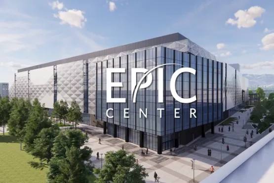
Applied’s $5 billion EPIC (Equipment and Process Innovation and Commercialization) Center, the largest U.S. investment in semiconductor equipment R&D, will serve as the primary collaboration site. The facility, operational later this year, is designed to compress the timeline from early-stage research to high-volume manufacturing by enabling faster learning cycles and earlier access to Applied’s R&D portfolio. For TSMC, this provides a secure environment to co-develop next-generation equipment and processes with direct input from Applied’s innovation teams.
Technical Focus Areas
The partnership will concentrate on three critical challenges in advanced logic scaling: new process technologies that deliver continuous power, performance, and area (PPA) improvements for AI and high-performance computing; novel materials and manufacturing equipment for precise formation of increasingly complex 3D transistor and interconnect structures; and advanced process integration methods to improve yield, variability control, and reliability as devices move toward vertically stacked architectures. These efforts directly target the growing demands of AI inference and training at both data center and edge deployments.
Market Context
This announcement underscores the industry’s shift toward deeper, pre-competitive collaboration as Moore’s Law scaling faces diminishing returns. By co-locating engineering teams, Applied gains multi-node visibility to guide its R&D investments, while TSMC accelerates technology readiness for its leading-edge nodes. The EPIC Center model represents a strategic response to the rising cost and complexity of semiconductor innovation, where traditional supplier-customer relationships are giving way to integrated co-development partnerships.
The partnership between Applied Materials and TSMC at the EPIC Center signals a new operational paradigm for semiconductor R&D, one that prioritizes co-location, shared risk, and accelerated commercialization. As AI workloads continue to drive demand for ever more energy-efficient compute, this collaboration will be instrumental in delivering the materials and process breakthroughs required to sustain the semiconductor roadmap through the next decade.