As AI accelerators push past multi-kilowatt power levels while operating voltages drop below 1V, resistive losses in traditional power delivery now waste 15 to 20% of total system power — hundreds of watts lost as heat before reaching the silicon.
The efficiency bottleneck
Modern AI systems face a fundamental physics problem: at sub-1V operating voltages, current demand scales dramatically, and resistive losses (I²R) grow with the square of that current. Traditional lateral power delivery routes power across the board, creating long, lossy paths between voltage regulators and the processor. For a multi-kilowatt AI accelerator, this translates directly into hundreds of watts dissipated as heat, compounding cooling requirements and straining data center infrastructure.
The industry has historically focused on processor efficiency and thermal management, but the power delivery path itself has become a major source of energy loss. Every watt lost between the rack and the chip is a watt unavailable for compute — a critical inefficiency as AI workloads scale.
Vertical power delivery gains traction
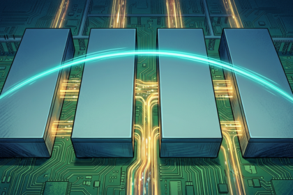
The industry is shifting from lateral to vertical power delivery architectures that place voltage regulation physically closer to the silicon. Shortening the power distribution path reduces resistive losses and improves overall system efficiency. This approach moves power delivery from a board-level afterthought to an integrated part of the package design.
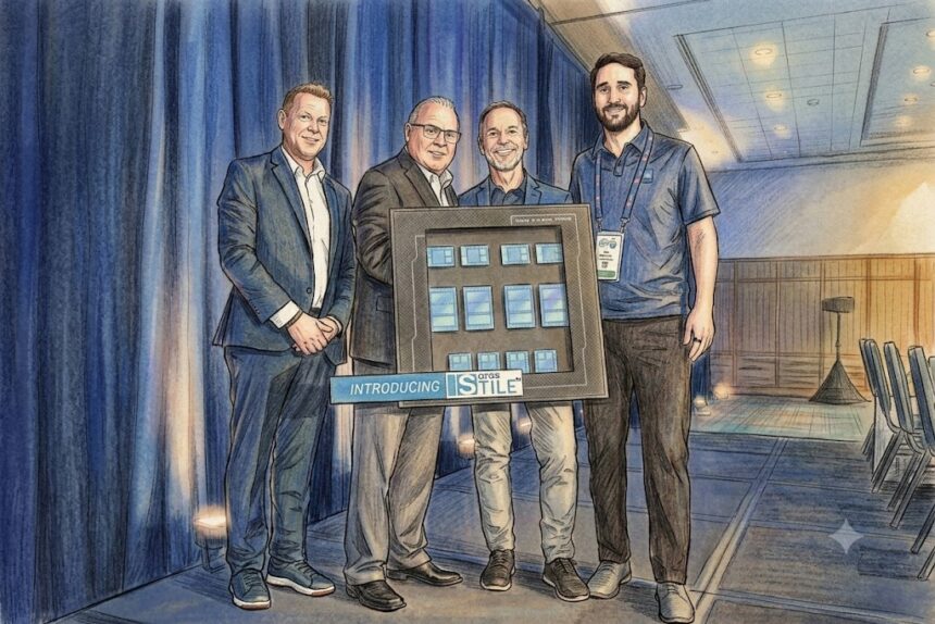
Saras Micro Devices’ STILE platform exemplifies this trend. It embeds passive functionality directly into the PCB and package structure — between the power module and the load device — supporting the regulation demands of modern AI accelerators while freeing board real estate for critical signal routing. Packaging discussions that once centered on interconnect density and thermal management are now evolving: packaging is becoming part of the power architecture itself.
Future architecture implications
Future package designs will incorporate increasing levels of package-integrated voltage regulation, embedded passives, and eventually some level of on-chip power conversion. This represents a fundamental shift in how the semiconductor industry approaches energy efficiency. The power delivery path must be evaluated as rigorously as processor performance and thermal management.
For enterprise data centers and hyperscale operators, the implications are clear: every percentage point of efficiency gained in power delivery directly reduces operational costs and enables higher compute density. The technology exists to address this challenge, but adoption will require close collaboration between chip designers, packaging engineers, and power system architects.
Conclusion
The next frontier in AI energy efficiency is not just in the processor — it is in the path that gets power to it. As AI accelerators continue to scale, vertical power delivery and package-integrated regulation will become essential infrastructure, not optional optimizations. The industry that masters this power path will unlock the next wave of sustainable AI compute.