Pushkar Ranade, Intel’s chief technology officer, was asked on the Dwarkesh Podcast whether unlimited money could lift worldwide leading-edge wafer output tenfold. Roughly double, he said, and that is the end of it.
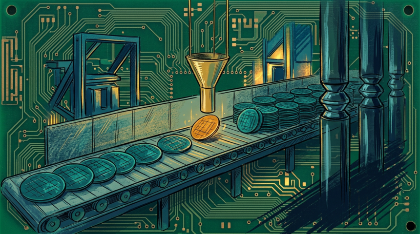
The ceiling he describes no longer sits with transistor design or with capital. It sits with the machines. ASML turns out under 100 extreme ultraviolet lithography systems in a year, with no signalled jump before the decade closes, which leaves that pool to be carved up among Intel, TSMC and the memory houses. Order a tool today and it shows up in about eighteen months, he added. A fresh fab shell does not contribute capacity until the decade runs out.
Ranade also took apart the idea that money alone buys more wafers. Adding buildings does not add output on its own, because power, water, consumables and clean room floor space can outrun the tools installed inside. Intel is helping speed Elon Musk’s fab build for that reason, telling him equipment, not cash, sets the pace.
Against that flat line, demand compounds at more than three times a year. Ranade expects a swing back toward vertical integration, with hyperscalers now big enough to consume a whole fab’s output.
The gap that is not about science
On Intel itself his verdict was blunt. Ranade puts the company a few percentage points from rivals on performance, power and density, and argues that hitting schedules with high yields counts for more than any design advantage. Fixed costs are about eighty percent of fab economics, so utilisation and yield settle who can afford the next tool order.
The equipment is already going in at Fab 62 in Arizona, a step Intel announced October 21, with production slated before the end of 2028. That is the lag Ranade described, arriving on schedule.