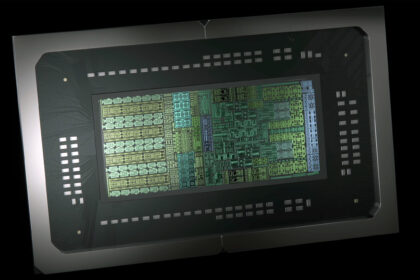

Groq, the inference chip company that licensed its technology to Nvidia, is looking at 3D stacked DRAM for its next generation of accelerators, according to reports from ZDNet Korea picked up by trade press.
The shift would be substantial. Groq’s current design puts everything in static memory. Each LPU carries 500MB of SRAM running at 150 terabytes per second, and a full 256-chip rack aggregates 128GB with some 640 terabytes per second of scale-up bandwidth.
SRAM is the fastest memory available on a die and the most expensive per bit. Its capacity grows slowly, roughly 10 to 20 percent every two years by one industry estimate, while the models these systems serve have been doubling on a much shorter cycle. That gap is the problem.
3D stacked DRAM, known as 3DS, connects memory dies vertically through silicon vias. It looks structurally like high bandwidth memory, but the two aim at different things. HBM chases bandwidth. 3DS chases capacity while keeping a conventional DRAM interface.
The trade is speed for room, and it would bring Groq closer to the mixed approach its parent already uses. Nvidia’s current LPX racks pair the SRAM with 12TB of DDR5 per rack, acknowledging that fast memory alone cannot hold a large context.
Manufacturing adds another dimension. Samsung builds the current Groq 3 LPU on its 4nm process at Pyeongtaek, giving the Korean foundry a foothold in inference silicon. Any move to stacked memory would deepen reliance on advanced packaging capacity, the same pool that HBM makers are already competing for.