Two Korean memory makers will use MICRO 2026 in Athens next month to argue over one question: how much of an AI workload can leave the GPU for the memory chips. The IEEE/ACM International Symposium on Microarchitecture runs from Oct. 31 to Nov. 4.
NELSSA is the SK hynix proposal, built with KAIST: an LLM serving system in which GPUs work beside processing-near-memory, or PNM, units. Traffic is sorted by request length, so short prompts stay on the graphics chip while long-context work moves to the memory side. A prototype wired over CXL reached as much as 5.5 times the decoding throughput of a GPU-only setup.
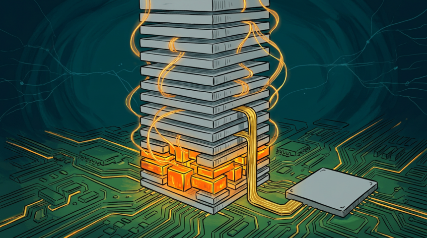
AMMA, Samsung’s entry, grew out of collaboration with researchers at UC San Diego, at Yonsei University and at Nvidia. The accelerator trades the GPU’s compute die for an HBM-centric layout that wraps logic and memory into one multi-chiplet package. Simulated against an H100, it cut inference latency to one sixteenth and energy use to one seventh.
Elsewhere on the program the same instinct holds. SK hynix researchers contribute C3, which partners a CPU with general-purpose DRAM, and DUALign, on placing data close to compute units. Samsung offers SYMPHONY, aimed at memory operations and communication scheduling for 3D DRAM accelerators.
The shared premise is simple: once context windows stretch into the hundreds of thousands of tokens, fetching data matters more than raw compute.