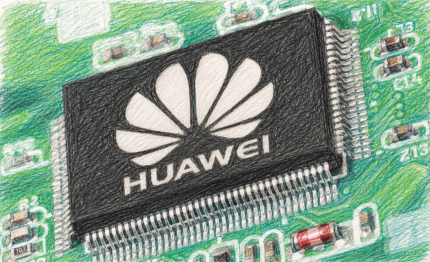
Huawei announced a novel chip design framework at the IEEE International Symposium on Circuits and Systems, claiming it can bypass US sanctions and deliver 1.4nm-class transistor density by 2031.
Breakthrough architecture
Huawei board member and HiSilicon President He Tingbo unveiled the proprietary “LogicFolding” architecture, built on a new “Tau Scaling Law.” Unlike traditional Moore’s Law geometric scaling—which relies on shrinking transistor physical dimensions using extreme ultraviolet (EUV) lithography machines—Tau Law is a temporal scaling framework. It prioritizes signal speed by optimizing data movement across the system rather than reducing component size.
LogicFolding physically folds and stacks logic circuits into a dual-layer structure. This drastically shortens internal wiring, eliminating signal delay. The result is a claimed 55% increase in transistor density and a 41% boost in power efficiency, enabling Huawei to produce competitive processors without restricted Western manufacturing equipment.
Commercial deployment timeline
Huawei revealed it has spent six years refining the methodology, secretly designing and mass-producing 381 chips based on the principle. The company will debut LogicFolding in flagship Kirin smartphone processors this autumn, likely in the Mate 90 series. By 2030, Huawei plans to scale the architecture to its Ascend AI processors and data center clusters, providing local alternatives to restricted Nvidia hardware. By 2031, the firm projects it can design chips with transistor density equivalent to a 1.4nm process.
Strategic implications
Huawei’s announcement comes as China aggressively invests in domestic alternatives to end reliance on foreign semiconductor players. Following the news, shares of China’s largest contract chipmaker, SMIC, surged 7.6%. While global foundry leader TSMC expects to mass-produce true 1.4nm chips by 2028, Huawei’s alternative path allows China to dramatically close the performance gap through innovative packaging and chip structuring, significantly mitigating the impact of US export controls.
This development represents a major symbolic and practical win for Beijing’s push toward technological self-sufficiency. If Huawei delivers on its claims, the semiconductor landscape could shift from a race for ever-smaller lithography to a competition in architectural innovation—fundamentally altering the rules of chip scaling and the effectiveness of technology sanctions.