
The April/May issue of *Semiconductor Digest* delivers a focused editorial lineup addressing critical inflection points across the semiconductor value chain, from advanced packaging and metrology to materials science and AI-driven manufacturing. This collection of articles provides actionable insights for engineering and operations leaders navigating yield, thermal management, and scaling challenges.
**Manufacturing and Yield Optimization**
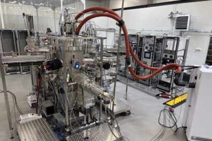
Two features examine non-destructive fault localization and precision sensing. Quantum diamond magnetic imaging offers a novel approach to electrical fault localization without compromising device integrity, while advanced X-ray inspection technology continues to push the boundaries of defect detection in high-reliability applications. Separately, a deep dive into Intel’s die sort and singulation operation underscores the often-overlooked importance of back-end processes in overall yield management. These articles collectively highlight how metrology and inspection are evolving to meet the demands of sub-5nm nodes and heterogeneous integration.
**Materials, Thermal Management, and Process Control**
Thermal interface materials based on silicone formulations are presented as a practical solution for improving data center cooling efficiency and chip-level thermal performance, a growing concern as power densities rise. In process control, valve selection for ultra-high-purity gas and chemical delivery remains a critical yet underappreciated factor in maintaining fab contamination standards. Separately, picosecond laser optimization for ABF (Ajinomoto Build-up Film) drilling addresses the precision requirements of advanced substrate manufacturing.
**Market and Strategic Considerations**
The issue includes several industry observations with strategic weight. One analysis questions whether power semiconductors are poised to become the next component crisis, mirroring recent supply chain disruptions. Another examines the shift from traditional PPA (power, performance, area) metrics to total cost of ownership as the driving force in chip design decisions. Additional pieces cover the scaling of pilot lines to high-volume manufacturing, the role of AI-driven rapid prototyping, and the intersection of water management with data center and fab operations.
**Conclusion**
This issue reinforces that the semiconductor industry is simultaneously managing near-term operational pressures—yield, thermal limits, and supply chain risk—while investing in long-term capabilities such as photonic interconnects, advanced memory architectures, and manufacturing-driven construction. For technology leaders, the common thread is the need for precision at every layer: from materials selection to metrology, from packaging to process scaling. The next wave of competitive advantage will belong to those who integrate these disciplines into a cohesive, cost-aware, and yield-focused strategy.