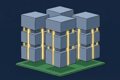
Researchers at the University of Seoul have proposed a hybrid memory design that tightly integrates DRAM and NAND flash to move data directly between the two, aiming at one of computing’s most stubborn bottlenecks.
The architecture, dubbed NAD memory, was detailed in a technical paper by Sojoong Kim and colleagues. Instead of shuttling data through a controller over standard interfaces, NAD enables parallel, cell-level transfer between DRAM and NAND, cutting the latency and energy spent on data movement.
Data movement now dominates the energy budget of modern systems, especially in AI workloads where models and weights constantly stream between storage, memory and compute. Hybrid schemes that let storage participate more directly in computation have become a major research thread, and NAD’s cell-level coupling is among the more aggressive proposals.
The paper, published through IEEE, argues the approach can improve both performance and efficiency compared with conventional SSD-plus-DRAM hierarchies, with implications for NVMe and PCIe-based systems. The team did not disclose a commercial timeline, and the work remains at the research stage.
Still, the concept lands at a moment when the memory industry is hunting for ways to flatten the hierarchy between volatile and nonvolatile memory, giving chipmakers another option to weigh as AI systems strain conventional storage paths.