The packaging lines that assemble AI accelerators have become the industry’s newest bottleneck, and TSMC is reportedly preparing a second tool for the job.
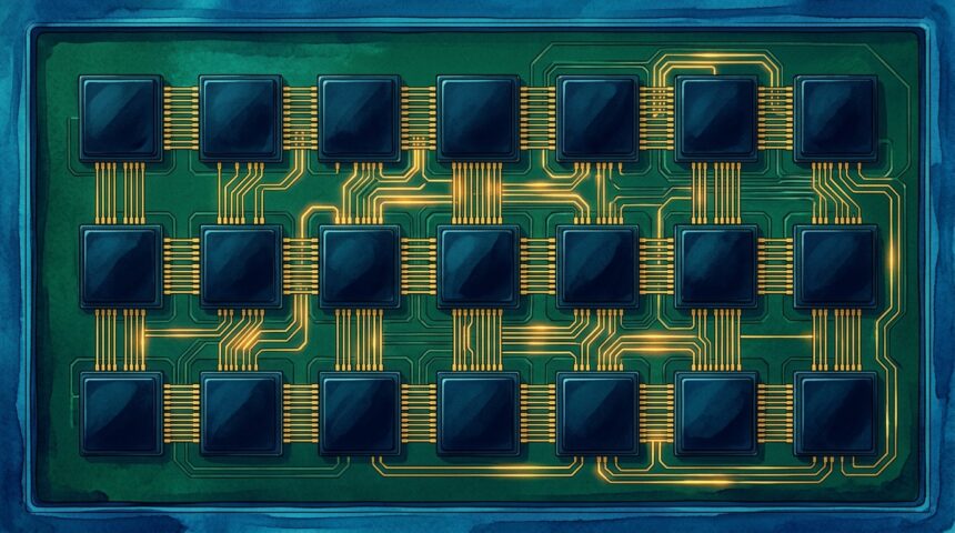
The foundry is said to be working with Kinsus Interconnect Technology, a Taiwan substrate specialist, on a system its engineers call quasi-EMIB. The concept echoes Intel’s Embedded Multi-Die Interconnect Bridge, which hides small silicon bridges inside the package substrate so chiplets can exchange data at high speed without a full interposer.
CoWoS, TSMC’s flagship packaging platform, underpins AI accelerators from NVIDIA and AMD. It has been oversubscribed for months, and the shortage has become a production ceiling: even with enough finished wafers, chipmakers cannot ship systems faster than packaging capacity allows.
A less elaborate alternative could help. Simplifying the bridge structure would mean fewer process steps, shorter cycle times and lower per-unit cost, though TSMC and Kinsus have not disclosed bridge geometry, interconnect density or any production schedule. Industry observers caution that quasi-EMIB remains an internal project name rather than a confirmed product line, and it may target midrange designs that do not need CoWoS’s extreme density.
The timing matters as much as the technology. Intel has spent years marketing EMIB as a differentiator in its foundry pitch, and TSMC building its own version shows how fiercely packaging leadership is now contested. A growing share of the AI boom’s profit will be decided at the substrate level.