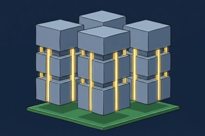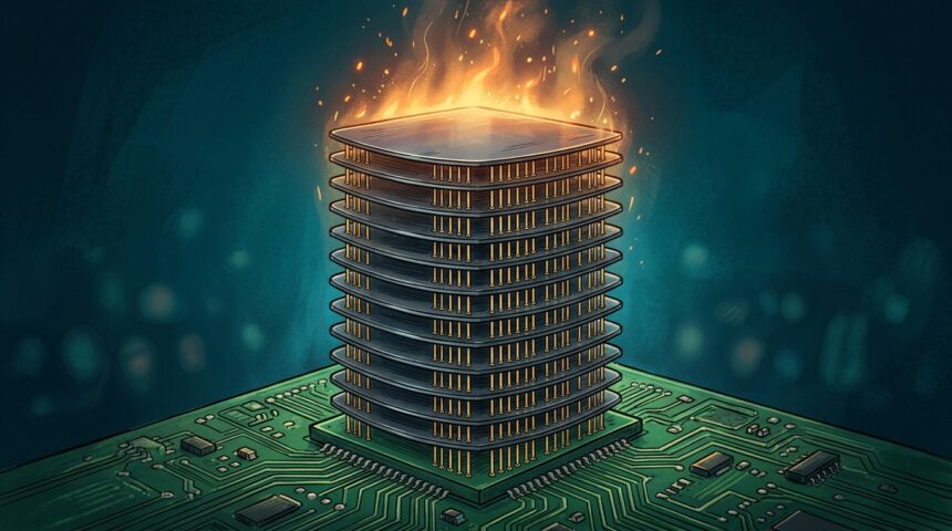
Stacking more layers in an HBM module is running into hard physics, according to a SemiEngineering analysis drawing on Hot Chips 2026 talks. Micron, Samsung, and SK hynix are adding dies to meet AI bandwidth demand, but each layer brings new failure modes.
Each additional layer means DRAM dies must be ground thinner to fit inside package height budgets. Thinner dies handle badly in manufacturing and packaging, warp more easily, and concentrate power density, lengthening the thermal path through the stack. Underfill voids and misalignment defects can scrap an entire cube.
Through-silicon vias remain the main data path, and more TSVs mean more bandwidth. But vias consume die area, cutting the data each layer can store, while taller stacks complicate packaging and heat removal that starts at the logic die.
Jim Handy of Objective Analysis told Hot Chips that AI spending, the demand for bandwidth, and HBM’s wide buses explain today’s DRAM shortage. Samsung’s Sangwook Han noted bandwidth has doubled every generation, leaving TSVs between dies as one of two bottlenecks.
Because HBM burns more silicon and wafer capacity per bit than commodity DRAM, these yield problems feed directly into supply at a moment when memory prices are already climbing.