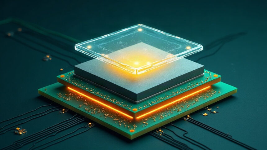
SK hynix says it has validated HBM5 on TSMC’s Chip on Wafer on Substrate packaging, the 2.5D process that places memory stacks beside a GPU on one interposer.
The work earned the company Partner of the Year honours in the 3DFabric-HBM Integration category at TSMC’s Open Innovation Platform conference in Santa Clara, its second consecutive win in that slot.
Each HBM generation adds layers and speed, but the gain only reaches an accelerator if packaging keeps pace. SK hynix has used the forum since 2024 to show memory developed jointly with the foundry.
At its booth the company displayed Nvidia’s next superchip, Vera Rubin, fitted with 12-layer 36GB HBM4 and 96GB SOCAMM2 modules. Other parts on show included 12-layer 48GB HBM4E, 16-layer 48GB HBM4 and 192GB SOCAMM2.
For servers it showed a 256GB 3DS RDIMM, a 128GB MRDIMM and a 64GB RDIMM, plus two enterprise SSDs, one supporting direct liquid cooling and a first quadruple-level cell drive.
An SK hynix executive said the PCIe SSD market should grow almost fourfold by 2030, and that the company will split SSD controller functions across chiplets linked by UCIe from PCIe Gen 6 onward.