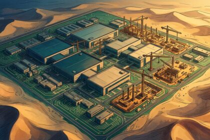

Samsung’s oldest semiconductor site is about to host its newest process technology. The Korean group will place foundry lines for 2-nanometer and 4-nanometer class chips at Giheung, the Yongin campus that opened in 1983, after clearing the ground last month. The main fab block will share the site with a green building and a substation, all bundled under the Project Kairos name. Samsung E&A takes engineering, procurement and construction, working in four production phases as at the newer Pyeongtaek plant.
The logic is HBM economics. Memory output on a bit basis is forecast by the industry to climb an average 52% annually through 2028 as hyperscalers place larger orders. Samsung builds HBM4 core dies at Hwaseong and Pyeongtaek, yet base dies, made on 4-nanometer tools, come from only a portion of the lines there. Leading-edge capacity closer to the research center lets base die supply keep pace.
The 2-nanometer segment serves a further purpose. HBM5, due to enter production next year, is expected to need base dies on the finer node, so early Kairos phases lay groundwork.
Cost estimates are large. Kairos alone runs near 25 trillion won. Internal quotes cover several dozen extreme ultraviolet scanners at roughly 8 trillion to 10 trillion won, and cleanrooms plus other tools push the total past 20 trillion won. Turning part of Line 6 into a packaging facility, where dies are stacked into finished HBM, could add enough to bring the bill toward 30 trillion won.
Ancient lines will sit alongside. Line 6 handles 8-inch wafers for image sensors and power parts, while Line S1 makes mobile processors on 12-inch wafers.