ASML built its lithography empire on immersion and extreme ultraviolet scanners, but a new SemiWiki analysis argues the next shift may come from tools that skip the mask entirely.
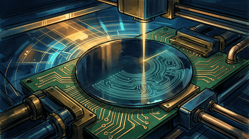
Instead of projecting a reticle pattern, maskless machines write chip layouts directly from digital files, using electron or ion beams, scanned lasers, or tiny micromirror arrays. The appeal is economic: EUV reticles carry heavy correction costs that climb with every node, while direct writing carries no reticle bill. The tradeoff is speed, since serial writing cannot match the throughput of optical replication.
The analysis sees the transition starting small. Multi-beam systems already help produce the masks EUV scanners depend on, and direct write looks best suited to mask repair, prototyping, and low-volume custom layers rather than leading-edge logic.
For now, ASML’s optical replication lead looks secure at the high end. A maskless challenger would need to match nanometer resolution, overlay accuracy, defectivity, and hundreds of wafers per hour to compete on cost per correctly patterned layer, a bar that includes yield learning and cycle time, not just headline resolution.
The timing is notable because the industry’s two biggest customers are split on how to proceed: Intel is pushing High-NA EUV into production while TSMC waits for the economics to improve, keeping ASML central to both strategies.