AMD announced a $10 billion investment in Taiwan’s semiconductor ecosystem to scale AI chip and server production, signaling sustained hyperscaler demand.
Strategic Investment in Taiwan
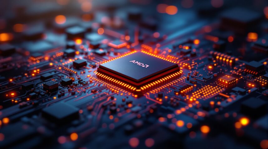
The investment targets TSMC’s 2-nanometer process node, where AMD has begun production of its sixth-generation EPYC CPUs, codenamed Venice. These are the industry’s first high-performance computing (HPC) chips to enter manufacturing on 2 nm. AMD CEO Lisa Su stated the move combines AMD’s HPC leadership with Taiwan’s manufacturing ecosystem to deliver rack-scale AI infrastructure at speed.
Hyperscalers are projected to spend up to $700 billion on data centers in 2026, according to McKinsey. AMD’s investment aligns with this trajectory, aiming to accelerate deployment of next-generation AI systems for global customers.
Manufacturing and Capacity Constraints
TSMC is struggling to keep pace with surging AI chip demand. The foundry expects to spend nearly $56 billion this year on capacity expansion but acknowledges it will likely fall short of demand until 2027. TechInsights vice chair Dan Hutcheson noted that wafer fab equipment supplier constraints and limited available “white space” are key bottlenecks, despite record tool shipments approaching $150 billion in 2026.
AMD is broadening its manufacturing partnerships beyond TSMC. The company is working with Taiwan-based chip packagers ASE and SPIL to develop next-generation 2.5D bridge interconnect technology, called elevated fanout bridge (EFB). This packaging method connects compute chiplets and memory on a single substrate, improving bandwidth and power efficiency in Venice CPUs. ASE expects its advanced packaging sales to double this year as traditional packagers fill gaps left by TSMC’s constrained CoWoS capacity.
Platform-Level Integration and Efficiency
AMD’s investments target system-level efficiency gains. The company qualified the industry’s first 2.5D panel-based EFB interconnect with Taiwan’s Powertech Technology, enabling high-bandwidth interconnect at scale. As AI chip surface areas exceed reticle sizes, wafer-level packaging on square substrates is replacing traditional round wafers.
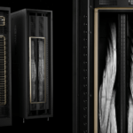
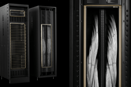
The AMD Helios rack-scale platform, powered by Instinct MI450X GPUs and EPYC CPUs, is scheduled for deployment in the second half of 2026. Contract manufacturers including Sanmina, Wiwynn, Wistron, and Inventec are building Helios-based systems, marking a shift toward production-ready AI infrastructure.
Forward-Looking Significance
AMD’s $10 billion commitment underscores that the AI infrastructure buildout is far from peaking. By deepening ties with TSMC, ASE, and other Taiwan-based partners, AMD is securing access to leading-edge nodes and advanced packaging capacity. However, persistent supply chain constraints across foundry, packaging, and equipment sectors will continue to shape the pace of AI deployment through 2027. The industry’s ability to scale manufacturing—not just design—remains the critical bottleneck.