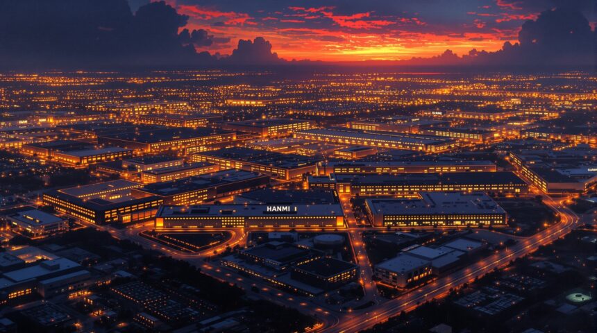
HANMI Semiconductor will enter the U.S. market through a new subsidiary in San Jose by late 2026, positioning itself to capture surging demand from AI-driven advanced packaging.
Strategic expansion into the u.s.
HANMI Semiconductor announced plans to establish HANMI USA in San Jose, California, by the end of 2026. The subsidiary will serve as an integrated operational hub, deploying skilled engineers to provide in-person technical support aligned with the construction schedules of new U.S. fabs. This move responds to the accelerating buildout of AI semiconductor production facilities, fueled by the CHIPS and Science Act.
The company expects a significant earnings increase starting in Q2 2025, driven by concentrated orders for its TC Bonders as mass production of HBM4 memory gains momentum. Chairman Kwak Dong-shin noted that the trend will accelerate in the second half of the year, with HANMI’s leading global market share in TC Bonders delivering outsized benefits as the AI semiconductor market expands.
Market context and customer demand
Major U.S. semiconductor projects are creating substantial demand for advanced packaging equipment. Intel’s Chandler, Arizona, foundry began operations in Q4 2025; Micron is building DRAM and HBM facilities in Idaho and New York; Amkor Technology will operate a large packaging plant in Phoenix by 2027; SK hynix plans an advanced packaging facility in Indiana by 2027; and Elon Musk’s “Terafab” project in Austin, Texas, a $119 billion initiative targeting 1 terawatt of AI semiconductor output annually, is expected to generate explosive demand for packaging equipment.
The U.S. subsidiary also enables direct collaboration with hyperscalers such as Microsoft, Google, Amazon, and Meta. As these companies develop proprietary AI chips, they increasingly specify core packaging equipment, driving demand for HANMI’s solutions.
Product portfolio and revenue diversification
HANMI holds the top global market share in TC Bonders, essential for HBM manufacturing. The company plans to release a second-generation Hybrid Bonder prototype within the year. It is diversifying revenue through several product lines: 2.5D TC Bonders for foundries and OSAT companies, the world’s first BOC COB Bonder now shipping to global memory firms, and the EMI Shield 2.0 X series supplying aerospace customers, a market where HANMI has maintained leadership since 2016.
Forward-looking conclusion
HANMI Semiconductor’s U.S. entry marks a strategic pivot to align with the reshoring of advanced semiconductor production. By establishing a local presence, the company positions itself to capture sustained revenue growth from new fabs, hyperscaler partnerships, and expanding AI packaging demand. The move reinforces its role as a critical equipment supplier in the evolving global supply chain.