Two of the equipment industry’s closer collaborators are formalizing a deeper tie-up as AI systems push packaging toward the center of chipmaking.
Besi will become an innovation partner at Applied Materials’ EPIC Center, a research complex in Silicon Valley that Applied has billed as its largest-ever US investment in tool and process development. The Dutch company already shares a Singapore development site with Applied, and the pair have worked together since 2020 on the bonding technique that stacks dies directly, without solder.
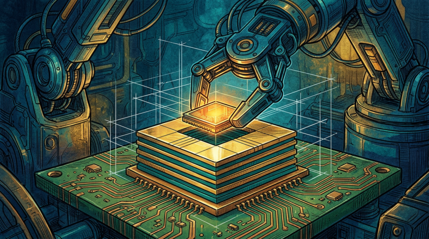
The new arrangement widens the field of play. Where the earlier work centered on that direct-bonding method, the companies now aim at the broader set of connections that carry signals between chips and into the package around them. Work is expected to span assembly done at the panel level along with newer thermal-compression and pick-and-place techniques.
Besi engineers will sit with Applied’s teams. Applied argues that packaging can no longer be treated as a finishing step bolted onto the back end, because the tight tolerances and cleanliness that bonding and panel integration demand look more like front-end wafer work.
Applied chief executive Gary Dickerson called Besi a trusted partner and said the expanded role carries the relationship into the interconnect technologies customers need for larger AI systems. Besi’s Richard Blickman said the long-running Singapore center had been central to its own bonding roadmap.